Motherboard 2 Digit BIOS POST codes in hex: Difference between revisions
ObamaMamma (talk | contribs) Created page with 'There are devices sold that are supposed to display a bios POST code in hex format based on the stage in bootup the BIOS POST is at. For example, a BIOS POST code of 01 means tha...' |
No edit summary |
||
| Line 7: | Line 7: | ||
[[File:Pci-usb-parallel-post-diagnostic-card.jpg]][[File:Pci-post-diagnostic-card.jpg]] | [[File:Pci-usb-parallel-post-diagnostic-card.jpg]][[File:Pci-post-diagnostic-card.jpg]] | ||
[[Category:Software]] | |||
Latest revision as of 15:46, 25 July 2015
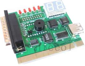
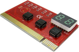
There are devices sold that are supposed to display a bios POST code in hex format based on the stage in bootup the BIOS POST is at. For example, a BIOS POST code of 01 means that processor 1 is being tested. Most of the POST diagnostic cards have 2 digit readouts, corresponding to the list of codes below.
Some of these motherboard POST diagnostic tools are based off of the PCI slot (also known as EISA). Other cards have the PCI slot AND a parallel port + USB port (used in conjunction), which allows for most laptops to be tested.
Some of the cards that use these codes:
POST Diagnostic Hardware Usage
- Power down the computer
- Plug in the POST diagnostic card
- For the PCI version, just plug into PCI slot
- For the USB/Parallel version, plug both USB and parallel in (not the PCI part)
- Power up and read the codes
POST Diagnostic Hex Codes
The code simply shows you where the computer is in its startup process. It is the most general codes for general POST and BIOS setups. These POST hex codes will be correct for most computers
|
Code |
Meaning |
|
01 |
Processor test 1: Verify CPU status flags?aset, test, clear, and test the carry, zero, sign, overflow flags (fatal) |
|
02 |
Processor test 2: Write/read/verify all CPU registers, except SS, SP and BP with data patterns FF and 00. |
|
03 |
Calculate BIOS EPROM and sign-on message checksum; fail if not 0 |
|
04 |
Test CMOS RAM interface and verify battery power Is available. |
|
05 |
Initialize chips: Disable NMI, PIE, AIE, UEI, SQWV; disable video, parity checking, and DMA: reset math coprocessor, clear all page registers and CMOS RAM shutdown byte: Initialize timers 0, 1 and 2, and set EISA timer to a known state: initialize DMA controllers 0 and 1: initialize interrupt controllers 0 and 1; initialise EISA extended registers. |
|
06 |
Test memory refresh toggle to ensure memory chips can retain data. |
|
07 |
Set up low memory; Initialize chipset early; test presence of memory; run OEM chipset initialization routines, clear lower 256K of memory; enable parity checking and test parity in lower 256K; test lower 256K memory. |
|
08 |
Setup interrupt vector table; initialize first 120 interrupt vectors with SPURlOUS_INT_HDLR and initialize INT 00-1F according to INT_TBL. |
|
09 |
Test CMOS RAM checksum and load default; if checksum is bad. |
|
0A |
Initialize keyboard; detect type of keyboard controller (optional); set NUMLOCK status. |
|
0B |
Initialize video interface; read CMOS RAM location 14 to find out type of video in use; detect and initialise the video adapter. |
|
0C |
Test video memory; write signon message to screen. |
|
0D |
OEM specific?ainitialise motherboard special chips as required by OEM; initialise cache controller early, when cache is separate from chipset. |
|
0E |
Reserved. |
|
0F |
Test DMA controller 0 with AA, 55, FF, 00 pattern. |
|
10 |
Test DMA controller 1 with AA, 55, FF, 00 pattern. |
|
11 |
DMA page registers?ause 1/O ports to test address circuits. |
|
12-13 |
Reserved |
|
14 |
Test 3254 timer 0 counter 2. |
|
15 |
Verify 8259 interrupt controller channel 1 by toggling interrupt Iines off/on. |
|
16 |
Verify 8259 interrupt controller channel 2 by toggling interrupt lines off/on. |
|
17 |
Test stuck 8259 interrupt bits: turn interrupt bits off and verify no interrupt mask register is on. |
|
18 |
Test 8259 functionality: force an interrupt and verify the interrupt occurred. |
|
19 |
Test stuck NMI bits (parity I/O check): verify NMI can be cleared. |
|
1A-1E |
Reserved. |
|
1F |
Set EISA mode: If EISA non-volatile memory checksum is good, execute EISA init. If not, execute ISA tests and clear EISA mode flat. Test EISA config mem checksum and communication ability. |
|
20 |
Initialize and enable EISA slot 0 (system board). |
|
21-2F |
Initialize and enable EISA slots 1-15. |
|
30 |
Size base memory from 256-640K and test with various patterns. |
|
31 |
Test extended memory above 1Mb using various patterns. Press Esc to skip. |
|
32 |
If EISA mode flag set, test EISA memory found during slot initialization. Skip this by pressing Esc. |
|
33-3B |
Reserved. |
|
3C |
Verify CPU can switch in/out of protected, virtual 86 and 8086 page modes. |
|
3D |
Detect if mouse is present, initialize it, and install interrupt vectors. |
|
3E |
Initialize cache controller according to CMOS RAM setup |
|
3F |
Enable shadow RAM according to CMOS RAM setup or if MEM TYPE is SYS in the EISA configuration information. |
|
40 |
Reserved |
|
41 |
Initialise floppy disk drive controller and any drives. |
|
42 |
Initialise hard disk drive controller and any drives. |
|
43 |
Detect and initialise serial ports. |
|
44 |
Detect and initialize parallel ports. |
|
45 |
Detect and initialise math coprocessor |
|
46 |
Print Setup message (press Ctrl-Alt-Esc to enter Setup at bottom of the screen, and enable setup. |
|
47 |
Set speed for boot. |
|
48-4D |
Reserved. |
|
4E |
Reboot if manufacturing POST loop pin is set. Otherwise, display any messages for non-fatal POST errors; enter setup if user pressed Ctrl-Alt-Esc. |
|
4F |
Security check (optional): Ask for password. |
|
50 |
Write all CMOS RAM values back to CMOS RAM, and clear the screen. |
|
51 |
Preboot enable: Enable parity, NMI, cache before boot. |
|
52 |
Initialize ROMs between C80000-EFFFF. When FSCAN enabled, init from C80000 to F7FFF. |
|
53 |
Initialize time value at address 40 of BIOS RAM area. |
|
55 |
Initialize DDNIL counter to NULLs. |
|
63 |
Boot attempt: Set low stack and boot by calling INT 19. |
|
B0 |
Spurious interrupt occurred in protected mode. |
|
B1 |
Unclaimed NMI. If unmasked NMI occurs, display "Press F1 to disable NMI, F2 to boot". |
|
BF |
Program chipset: Called by POST 7 to program chipset from CT table. |
|
C0 |
OEM specific?aTurn on/off cache. |
|
C1 |
OEM specific?aTest for memory presence and size on-board memory. |
|
C2 |
OEM specific?aInitialize board and turn on shadow and cache for fast boot. |
|
C3 |
OEM specific?aTurn on extended memory DRAM select and initialize RAM. |
|
C4 |
OEM specific?aHandle display/video switch to prevent display switch errors. |
|
C5 |
OEM specific?aFast Gate A20 handling. |
|
C6 |
OEM specific?aCache routine for setting regions that are cacheable. |
|
C7 |
OEM specific?aShadow video/system BIOS after memory proven good. |
|
C8 |
OEM specific?aHandle special speed switching. |
|
C9 |
OEM specific?aHandle normal shadow RAM operations. |
|
D0-DF |
Debug: available POST codes for use during development. |
|
EO |
Reserved. |
|
E1-EF |
Setup pages: E1 = page 1, E2 = page 2, etc. |
|
FF |
If no error flags such as memory size are set, boot via INT 19?aload system from drive A, then C; display error message if boot device not found. |
External Resources
- Generic POST Codes - Simple BIOS POST codes in hex format with descriptions
- PDF manual - OEM specific hex POST codes for POST motherboard diagnostic cards
- Most comprehensive list of POST hex codes for all makes and models of motherboards
- AMIbios post codes - List of hex POST codes for diagnostic cards
- Dell POST codes - Hex and beep codes for Dell motherboards
- AwardBIOS POST codes - Hex and beep codes for POST on AwardBIOS based bios
- HP BIOS POST codes - Hex POST codes and beep codes for HP motherboards
- Phoenix BIOS POST codes - Hex POST codes for Phoenix Bios motherboard diagnostics
- IBM BIOS POST codes - For IBM computers using IBM bios, hex POST codes

